CATV MAX3509 + 68dBmV cable telephone upstream communication scheme
Important: To improve the output signal of the MAX3509 cable upstream amplifier to support circuit-switched telephone systems, this application note gives specific design modifications. The amplifier has sufficient gain to provide 66dBmV output. This article discusses issues such as output echo suppression, heat dissipation, and harmonic distortion in detail.
For more information, please check:
The circuit-switched cable telephone system requires a large upstream signal to overcome the coupler loss (Figure 1). The MAX3509 can drive high output power while maintaining low harmonic distortion and complying with the Cable Data Service Interface Specification (DOCSIS). The circuit shown in Figure 4 has made some modifications to the MAX3509 evaluation board for high-power driving.
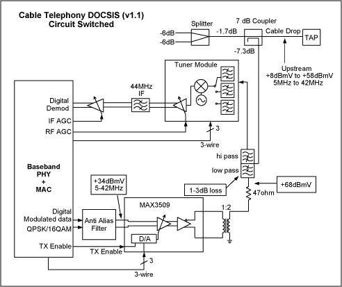
Figure 1. Structure diagram of cable phone
MAX3509 is a programmable power amplifier used in CATV upstream systems. This chip uses a 3-wire serial bus to control the gain, the gain control level difference is 1dB, and the operating frequency range is 5MHz to 65MHz. The MAX3509 has a prohibited-transmit mode, which puts the chip in a highly isolated state between bursts of the TDMA system. In this mode, all analog functions are turned off, reducing output noise and power loss. When entering or leaving the prohibited launch state, the transient response is kept at 25mV in the full gain range. In addition, the power supply current drops to 7.8mA.
When using an instrumentation amplifier configuration, the power amplifier provides two current feedback amplifiers. This structure has extremely low even-order harmonic distortion, but requires the conversion of a single-ended signal output through an external transformer. In the transmit inhibit mode, the power amplifier bias is minimized, providing higher input-output isolation and extremely low output noise.
Driven by an input signal of 34dBmV, the MAX3509 can provide sufficient gain to produce an output of 66dBmV (1: 1 transformer). Under this input level, the rated index can be reached. When the input level is reduced, the maximum output level is reduced and the output linearity is improved. If the input level is higher than 34dBmV, the distortion will increase.
On the upstream channel of 5MHz to 42MHz, DOCSIS requires 6dB echo suppression. This requirement is easily met when a coupler is used. For a 7dB coupler (Figure 1), regardless of the output impedance of the upstream amplifier, the echo suppression can be up to 14dB.
The MAX3509 has an output impedance of 1.2Ω in transmit mode and 170Ω in transmit inhibit mode. This output impedance is converted by a MAX3509 output transformer with an impedance ratio of 1: 4 (N = 1: 2 voltage) (in this case, Toko 458PT-1087 can be used). The equivalent source impedance and output transformer of the MAX3509 can be calculated according to Figure 4. In transmit mode, the output impedance of 1.2Ω is converted to 4.8Ω, which is 51.8Ω in series with a 47Ω resistor. In the emission inhibit mode, the output impedance of 170Ω is converted to 680Ω, which becomes 727Ω in series with a 47Ω resistor.
The current feedback amplifier will drive enough current to maintain the output voltage, which is beneficial to obtain low distortion under dynamic loads. Of course, low-impedance loads draw more current from the amplifier, so power consumption and heat dissipation must be considered. The first component of a duplex filter is a bypass capacitor, which reduces the output load impedance and increases the current draw. The low-impedance upstream amplifier can provide a good drive in the 42MHz band of the duplex filter.
The MAX3509 has a continuous power dissipation of 2200mW at + 70 ° C, and decreases by 27mW / ° C when it exceeds 70 ° C. This data is based on JEDEC PCB board. The maximum ICC is reduced when using the JESD51-7 PCB board. At 85 ° C and VCC = 9V, the maximum ICC is: (2200-(85-70) 27) / 9 = 199mA.
When the circuit board layout and output load are fixed, it is possible to safely increase the maximum current draw (Icc) using heat sinks. The maximum junction temperature of the MAX3509 is limited to + 150 ° C Θjc = 2.43 ° C / W. 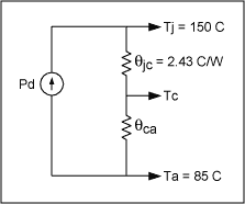
Figure 2 Power dissipation
For example: If the MAX3509 is known to output 230mA at 42MHz, 70dBmV output and the operating environment is 85 ° C, the following formula can be used to calculate the heat sink requirement:
Find Pd = VCC × ICC = 9V × 230mA = 2070mW, calculate Θjc + Θca = (Tj-Ta) / Pd = (150-85) /2.070 = 31.4C / W, then subtract Θjc from this value to get Θca = 28.97C / W. Θca is the heat dissipation of the heat sink. The heat sink is usually designed according to the surrounding metal base plate, where 95% of the heat is dissipated through the exposed pad at the bottom of the MAX3509. If the heat dissipation surface under the exposed pad is directly in contact with the heat sink, a higher heat dissipation efficiency will be obtained. In addition, adding a via between the heat dissipation surface and the ground plane can effectively increase the heat dissipation surface and help heat dissipation. Measuring the temperature value (Tc) of a specific application can ensure an appropriate heat sink design, and measure the temperature as close to the exposed pad as possible. Note that the thermal conductivity at the top of the MAX3509 is very small. If the heat sink is placed on top of the device, it will not produce effect.
There are three basic methods for reducing the power consumption of the MAX3509.
This design uses the above three methods. First, reduce the output power to + 67dBmV (see Figure 6). Second, connect a 47Ω output resistor in series to increase the output impedance. Third, the data is taken from 8.3V (a diode conduction voltage drop lower than 9V), which can save 100mW of power without affecting harmonics (see Figures 10 and 11).
In order to ensure that the operating characteristics are not affected, the heat sink is the best choice.
The ultimate goal of system design is to comply with the DOCSIS standard, the main barrier of which is the requirement to suppress stray radiation. Figure 3 shows the DOCSIS specifications for suppressing spurious signal radiation. The most difficult working condition is to limit the radiated power of spurious signals in the frequency range of 54MHz to 60MHz and 60MHz to 88MHz at full power output (+ 58dBmV). It can be seen from Fig. 3 that the suppression parameters to be provided are 93dBc and 98dBc, respectively. The in-band (5 to 42MHz) spur suppression is -47dBc, and the amplifier usually provides in-band and out-of-band harmonic suppression of -50dBc. Use a duplex filter to attenuate in-band harmonics. In order to design a duplex filter, you need to know the second and third harmonic distortion parameters of the upstream amplifier (MAX3509), and then combine the system specifications (DOCSIS see Figure 3) to determine the design requirements of the duplex filter attenuation.
For differential, bipolar products like the MAX3509, third-harmonic distortion is a more critical constraint than second-harmonic distortion. The two critical points of third harmonic distortion are fo = 18MHz (54MHz third harmonic) and fo = 20MHz (60MHz third harmonic). 22MHz is close enough to the 18MHz and 20MHz frequency points in practical applications. Figure 6 shows the third harmonic distortion of 22MHz. 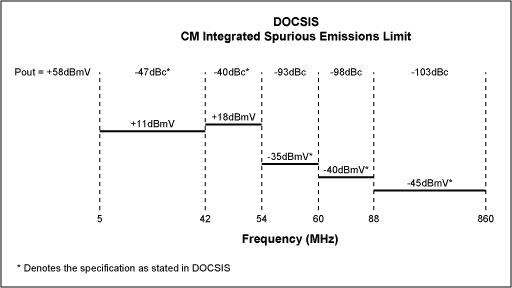
Figure 3. DOCSIS limits for spurious signal emissions
Figures 5 to 8 show the correspondence between harmonic distortion and output power when the input frequencies are 9MHz, 22MHz, 33MHz, and 42MHz, respectively. DOCSIS stipulates that the spurious signal should drop to -40dBmV or 98dBc (58--40) at the frequency of 60MHz. The MAX3509 has harmonic suppression of -53dBc at fo = 22MHz (the third harmonic at 66MHz) and Pin = 33dBmV (see Figure 6). The duplexer needs to provide 45dBc (98-53) attenuation at the 60MHz frequency point. The requirements for the duplexer in other frequency regions are: 54MHz frequency point DOCSIS stipulates that the spurious signal is within -35dBmV. When the input frequency is 18MHz, the corresponding third harmonic is 54MHz. The duplexer needs to provide 40dBc (58 + 35-53) insertion loss at 54MHz. It should be noted that the third harmonic distortion is a key factor. The best input power is 33dBmV or as low as possible.
All tests are conducted at room temperature.
Output transformer Toko 458PT-1087 N = 1: 2 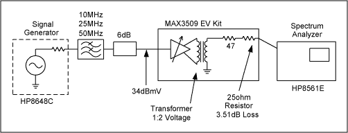
Figure 4. Test condition diagram
Figure 5 shows the second and third harmonic distortion data when the input is 9MHz fundamental frequency. The curve in the figure shows that the in-band harmonic characteristics are better than 59dBc when Pin = + 33dBmV (the third harmonic is limited to the linear range). This index is better than the 47dBc required by the DOCSIS specification. 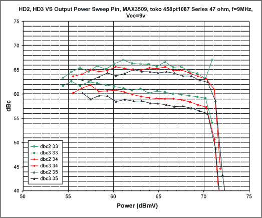
Figure 5.
Figure 6 shows the second and third harmonic distortion data when the 22MHz fundamental frequency is input. The curve in the figure shows that the in-band harmonic characteristics are better than 53dBc when Pin = + 33dBmV and Pout = + 67dBmV (the third harmonic is limited to the linear range). 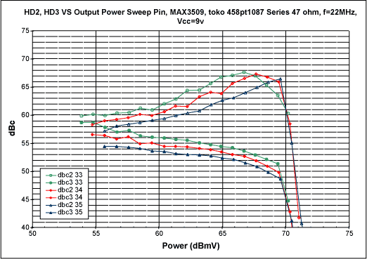
Image 6.
Figure 7 shows the second and third harmonic distortion data when the 33MHz fundamental frequency is input. The curve in the figure shows that the in-band harmonic characteristics are better than 51dBc at Pin = + 33dBmV and Pout = + 67dBmV (the third harmonic is limited to the linear range). 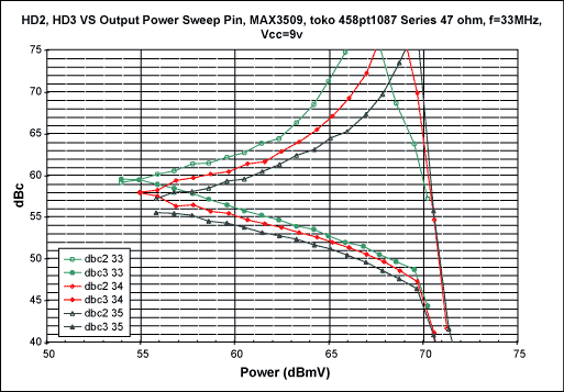
Figure 7.
Figure 8 shows the second and third harmonic distortion data when the 42MHz fundamental frequency is input. The curve in the figure shows that the in-band harmonic characteristics are better than 50dBc at Pin = + 33dBmV and Pout = + 67dBmV (the third harmonic is limited to the linear range). 
Figure 8.
Fig. 9 shows the data of the third harmonic distortion after hitting different input fundamental frequencies. The curve in the figure shows the third harmonic at different frequencies. 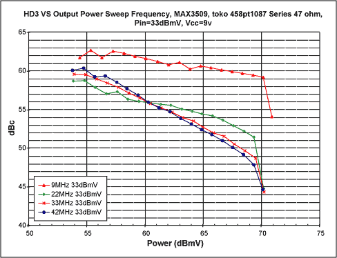
Figure 9.
Figure 10 shows the data changes of the third harmonic distortion when VCC is reduced to 8.3V. 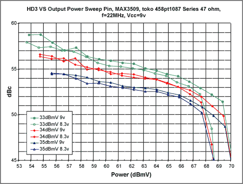
Figure 10.
Figure 11 shows that when VCC = 8.3V is used, 100mW of power can be saved. 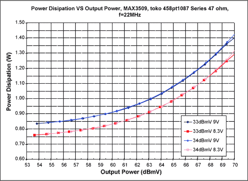
Figure 11.
Figure 12 shows that when VCC = 8.3V, 100mW of power can be saved. 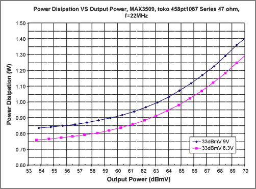
Figure 12.
Figure 13 shows that small changes in VCC do not affect ICC. 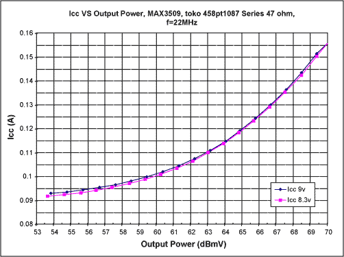
Figure 13.
The MAX3509 can overcome coupler losses (see Figure 4) and meet the power standards of the DOCSIS specification. The construction of this program includes the following steps:
The thermal test board descriptions given in this note are very consistent with Maxim IC applications.
Component surface wiring design: The leads need to be placed on the outside so that the test device is located in the center of the circuit board. The lead from the edge of the package must be at least 25mm longer. For packages with 0.5mm or wider spacing, the lead width should be 0.25 +/- 10%. For wider-spaced packages, the leads should be equal to the lead width. The lead pattern and lead endpoint must meet the specifications in JESD51-7.
Backside wiring design: Component side leads terminated with vias may be connected to the edge of the connector via leads or wires (22 AWG or smaller, copper wire). JESD51-7 specification specifies the current limit of different size wires.
Power plane and ground plane: In addition to the insulation clearance mode, the power plane and ground plane must be kept intact. And the power plane and ground plane cannot appear within 9.5mm of the connector edge. For other requirements, please refer to the detailed description in JESD51-7.
Phlizon specialize in Led Grow Lights for for various fields such as medical, government, military, commercial, and agriculture.More than 10 years experience research and development team focus on Grow Light .Many gained the National Patents,all products passed FCC and ETL certifications. We offer High quality with the most cost-effective price.


Phlizon grow bar series are the best solution for various urban farming systems., Full Spectrum Led Grow Light bars for plants growing,designed specifically for use as supplemental greenhouse lighting. Each bar 80W power.4 bars,6 bars ,8 bars 10 bars ,12 bars for choice.Adjustable bar quantity to make much more convenient repair and replacement in the future.Safety FCC ETL Certified and IP54 Rated.Passive cooling,extrusion pure aluminum can 100% ensure heat dissipation. Plants will grow better under the Full Spectrum Led Grow Lights, as well their yield. will increase hugely.
With a set of grow light bar, you can grow many plants indoors, including houseplants, orchids, and even some fruit and vegetable crops. Grow lights are ideal for seed starting because they help ensure stocky, green seedlings. A wintertime harvest of herbs and salad greens can also be grown under lights. By learning how plants use light and about the fixture options, you can select an indoor grow lights system that is right for the plants growing
Features:
High power brand Samsung 5630 led with high par vauleFull Spectrum Grow Light mimics natural sunlight for different period of growth
Customizable spectrum,any spectrum can be OEM/ODM,at any stage of growth accordingly
APP WIFI to make operation.Standard without dimming,dimming with different PPFD
Aluminum material and heat-dissipation design
Passive cooling,no fans,no noise
Energy saving,enviromental friendly
Adjustable bar quantity to make much more convenient repair and replacement
3-5 years Warranty

Hydroponics,Horticulture,Agriculture and Greenhouse
Locations:Farm,Exhibition,Garden,Home,Urban,Bonsai,and University Lab
Growth of Fruits,Vegetables,Flowers and so on
Seeding,Rooting,Breeding,Flowering and Fruiting period


PH Bar Series
Dimmable Led Grow Bars,640W Led Grow Light,Medical Flowers Grow Bars,Led Grow Light 8 Bars
Shenzhen Phlizon Technology Co.,Ltd. , https://www.philizon.com