1. The overall design of the electronic station card
This article refers to the address: http://
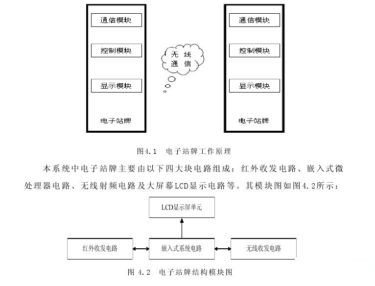
The so-called electronic stop sign] is a sign displayed in the form of an electronic screen. The electronic stop sign is a subsystem of the intelligent bus system, which presents the integration result of all functions and is the best medium for passengers to directly feel the convenience of the system. It integrates computer, communication and modern control technology, and is one of the symbols of urban bus informationization and modernization. It mainly completes two functions. First, it provides the passengers with the arrival information of the bus passing through the platform. For example, the current interval of the bus is about how long it takes to reach the station, changing the passengers waiting in the past. Passive waiting for the situation. Second, the communication connection with the adjacent station sign is completed, and the communication system of the station board is formed to form the entire bus system network. Figure 4.1 shows the working principle of the electronic station.
2, electronic station hardware design
The electronic station card mainly completes receiving information (including receiving of upstream station and arrival bus information), transmitting information, and displaying information. Its electrical block diagram is shown in Figure 4.3.
4.2.1 Microprocessor selection
Although the ARM microprocessors produced by each chip manufacturer are different, they are nothing more than the following series [33]: ARM7 series, ARM9 series, ARM9E series, ARM10E series, SecurCore series and Intel's StrongARM, etc. Serial Processor Processing In addition to the common features of the ARM architecture, each family of ARM microprocessors has its own characteristics and application areas. For example, ARM7 series is suitable for industrial control, network equipment, mobile phones and other applications; ARM9 series, ARM9E series and ARM10E series are more suitable for wireless devices, consumer electronics design; SecurCore series is designed for high security applications; Intel The StrongARM processor is ideal for portable communications products and consumer electronics.
From an application point of view, the following aspects should be considered when selecting a microprocessor [10][31]: The choice of 1 ARM core is well known. The ARM microprocessor contains many series of core structures for different application fields. For example, if users want to use Windows CE operating system to reduce software development time, they need to select ARM chip with MMU (Memory Management Unit) function above ARM720T, because ARM7TDMI does not have MMU and does not support Windows CE.
2ARM chip internal memory capacity
Most of the ARM microprocessor's on-chip memory is not too large, requiring the user to expand the memory while designing the system. However, some chips have relatively large on-chip storage space, and their own memory space can meet the engineering requirements, thus simplifying the system design.
3ARM chip on-chip peripheral circuit interface In addition to ARM microprocessor core, almost all ARM chips expand the relevant functional modules according to their different application areas, and integrated in the chip, which is the on-chip peripheral circuit. The designer should use the on-chip peripheral circuits to complete the required functions as much as possible according to the requirements of the project, which can simplify the design of the system and improve the stability of the system.
Starting from the feasibility of the study, the program uses the ARM7TDMI core of the ARM architecture. It is a widely used 32-bit embedded RISC processor, mainly used in low-end electronic devices. In addition, because ARM has extremely high instruction efficiency, extremely high clock frequency. Therefore, its computing power is very powerful, and its internal resources are also very rich. The hardware solutions with ARM microprocessor as the core are more mature and mature, which greatly simplifies the hardware design and shortens the development cycle.
The main tasks of the main control processor in this system include:
1 Receive the bus signal and the signals sent by other electronic station cards, and process them and send them to the electronic station display screen to show the vehicle arrival and vehicle driving conditions.
2 Then, the corresponding information is sent to the next station electronic stop card through the wireless module, and the information of the currently traveling vehicle of the entire route is dynamically displayed on different stop signs by the relay method, so that the entire line information is completed. Pass in real time.
Combined with the main task requirements of the system, considering the processor performance, price application prospects and other factors, Philip's LPC2214 chip becomes an ideal processor for this system. It integrates two UATR, I2C serial interface, SPI serial interface, general I/O port and other functional modules. It is also a 16/32-bit ARM7TDMI CPU microcontroller that supports real-time simulation and tracking. Very suitable for the development of terminal products.
4.2.2 Microprocessor LPC2214 Features
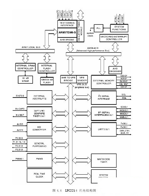
The LPC2214[8] microprocessor selected in this article is a 16/32-bit ARM7TDMI-S CPU based on real-time emulation and tracking. It has 256KB of high-speed flash memory, on-chip bit width interface and unique The accelerated architecture provides a hardware foundation for 32-bit code to run at maximum clock rates, while its 16-bit Thumb mode reduces code size by 30% with little loss of performance. The internal structure block diagram of LPC2214 is shown in Figure 4.4, and its characteristics are mainly [13]:
116/32-bit ARM7TDMI-S microcontroller;
216KB static RAM;
3256KB on-chip FLASH program memory, 128-bit wide interface/accelerator for operating frequencies up to 60MHz;
4LQFP144 foot package;
5 on-chip boot loader implementation in system programming (ISP) and in-application programming (IAP);
68-channel 10-bit A/D converter with conversion time as low as 2.44us;
72 32-bit timers (with 4 captures and 4 compare channels), PWM unit (6 outputs), real-time clock and watchdog;
More than 8 serial interfaces, including 2 16C550 industry standard UART, high speed I2C interface (400Kbps) and 2 SPI interfaces;
9 The CPU operating frequency of up to 60 MHz can be realized by the on-chip PLL;
10 vector interrupt controller. Configurable priority and vector address; 112 general purpose I/O ports (withstand 5V), 12 independent external interrupt pins (EINT and CAP functions);
? On-chip crystal frequency range: 1 ~ 30MHz;
Wake the processor from power-down mode with an external interrupt;
Optimize power consumption by individually enabling/disabling external functions;
? Dual power supply: CPU operating voltage range: 1.65 ~ l.95v (1.8V × (l ± 8.3%));
? I / O operating voltage range: 3.0 ~ 3.6V (3.3V × (1 ± 10%))
3 auxiliary circuit design
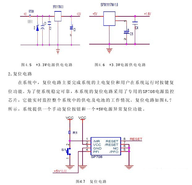
Power supply circuit
Because the LPC2214 microcontroller has two sets of power supplies, one is the I/O port power supply voltage is 3.3V, and the other is the core power supply voltage is 1.8V, so the system must have two sets of power supply voltage conversion circuits, the circuit is shown in Figure 4.5 And Figure 4.6, Figure 4.5 is a 3.3V power supply circuit, Figure 4.6 is a 1.8V power supply circuit.
After the number, the TSOP1738 receiver output pin will output a low level, otherwise the pin will output a high level, which can demodulate the “intermittent and continuous†infrared light signal into a continuous periodic square wave signal. The processor can recover the original data signal by processing the output signal of the TSOP1738 through the keyboard interrupt pin or the external interrupt IRQ pin. This article uses the external interrupt IRQ processing of the microprocessor.
4.2.5 Infrared receiving system software design
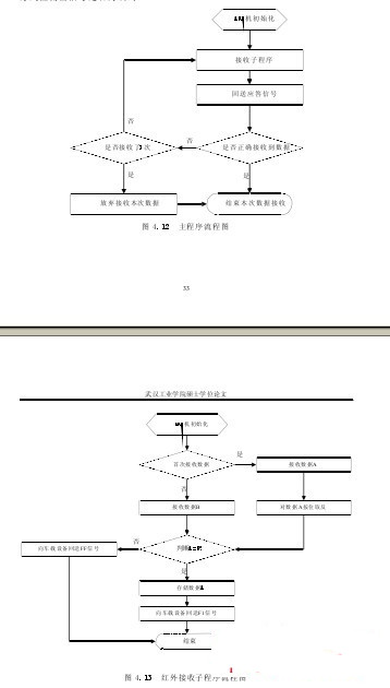
In the actual infrared communication process, in addition to random errors, there are often sudden errors. In infrared communication, sudden errors are often caused by light interference or continuous misalignment errors caused by dust particles and mist scattering and absorption of infrared rays in the air [36]. In the error interval, the symbol becomes all "0" or all "1". For such burst errors, the simple parity method can't do anything, but using data retransmissions can detect such errors. The microprocessor receiving subroutine flow chart is shown in Figure 4.12. The receiving end uses the received data twice to determine the correctness. When there is external interference, the probability of the opposite interference at the position corresponding to the normal data signal and its inverted code is extremely small. Therefore, the receiving end can utilize this method. It is detected whether the signal is an error.
4.2.6 Circuit Design of Wireless Communication System
Communication method
Generally speaking, the distance between the two bus stops in the city is about 1Km. If the information is transmitted by wire, there are many inappropriate places. One is that the cost of wiring is high and the maintenance cost is large. The second is that the city develops rapidly, the station often changes, and the communication link also changes, which will be very troublesome. Therefore, we consider the choice of wireless communication. Existing wireless communication methods include mobile communication networks, wireless modules, and the like. Due to the development of communication technology, the high-precision wireless communication module can basically meet the transmission distance between the existing bus stations. Under the premise that the basic can be satisfied, we prefer the wireless module transmission mode in the wireless communication mode. After all, the mobile communication network is rented, and the usage cost is relatively high. If the system is running and it is found that the wireless module transmission method cannot meet the requirements, we use the GSM short message method [38] as an alternative.
The reliability and effective communication distance of the wireless transceiver in this system is the key to the design [38][39]. For this reason, the system uses the SRWF-508[40] chip produced by Shanghai Sangrui Electronic Technology Co., Ltd. as the wireless receiver.
Hair device, it is a chip with a wide operating frequency. The SRWF-508 wireless data transmission module uses high-efficiency FEC forward error correction technology combined with high-performance wireless RF ICs and high-speed microprocessors to develop a first-line communication module. The wireless communication module provides an RS-232 interface, and can transmit wireless length data at a time, and the transmission distance can reach 4.5KM or more, based on the modulation mode of GFSK [39].
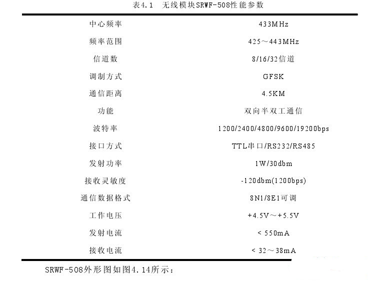
Efficient communication protocol, transparent data interface, can adapt to any standard or non-standard user protocol, automatically filter out noise signals and false data generated in the air, with strong anti-interference ability and low error rate. No coding technology is required, and good wireless data transmission can be accomplished without extending peripheral circuits. Its technical indicators are shown in Table 4.1 [40]:
In this system, the wireless transceiver module SRWF-508 is installed on each bus stop card, so each station transmits and receives information to and from each other through the module. At the same time, some downstream electronic station cards may receive the information of the upstream electronic station card. In order to prevent mis-transmission, we use the method of adding address identification to transmit [41], only the same electronic station as this address. Cards can receive information. The stop sign, the control center and the stop sign form a closed loop [41][42]. The terminal electronic station transmits the relevant vehicle operation information to the control center through the mobile wireless network, and the control center feeds back the information through the electronic terminal of each line terminal. Make appropriate adjustments to make the road unblocked.
2. The working principle of the communication module
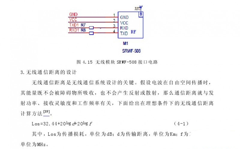
After the microprocessor transmits the data to the SRWF-508 by using the serial port mode, the SRWF-508 determines whether the received code stream is a command or a data, and if it is a command, executes the command, and if it is the data to be sent, the data to be sent is sent to the first transmission. Buffer, because the communication mode of the module is half-duplex communication, the module must be converted from the receiving state to the transmitting state. This conversion process is less than 10ms, and the packetizing program is started after the state conversion is completed. The function of the sending package program is to pack the data of the buffer into a data packet suitable for wireless transmission, and send the data of the data packet to the data modulation port in the module to be transmitted by the modulation mode of GFSK and its transmission frequency is 433 MHz. The transmission power is 30dB. When the antenna height is greater than 3m, the transmission distance can be as far as 4.5Km. The SRWF-508 module interface circuit is shown in Figure 4.15.
In this system, because the vehicle runs in both directions, the system uses two working frequencies to distinguish the vehicle's going and return. The SRWF-508's working frequency is 425MHz and 433MHz, the transmitting power is 30dB, and the receiving sensitivity is -120dB. -1) It can be calculated that the propagation distance is about 50Km under ideal conditions.
4.SRWF-508 working parameter test
The magnitude of the power loss has a crucial impact on the stability of a system, so we tested the relevant parameters. The working voltage of the wireless module is +5V, the working frequency is 433MHz, and the working environment temperature is about 18°. The test results are shown in Table 4.2. From the table, we can see that the module consumes less power during operation and stands by during sleep. The power consumption is lower.
Table 4.2 Wireless Module SRWF-508 Test Parameters
Parameter size
Receive current 27mA
Emission current 520mA
Sleeping current 21μA4.2.7 wireless transceiver system software design
1. Communication protocol format
In order to realize the transmission of information between stations, we must establish a set of suitable communication protocol standards, in order to facilitate the real-time transmission of information and ensure the normal operation of the network. The so-called communication protocol [39] [42] refers to an agreement between the two parties. The agreement includes uniform definition of data format, synchronization mode, transmission speed, transmission procedure, error detection mode, and control character definition. Both parties must comply with each other. In the communication protocol, the communication information format is very important, and the communication information can be roughly divided into the following two categories:
1 command information. It includes request commands, response commands, and control commands. In this system, the command information includes a request command and a response command.
2 data information. In the entire bus information service system, the main transmission is the vehicle location information, which is the useful data that the electronic station card actually needs to receive. For command information, the information format is:
Interference signals may be present during the transmission of information. If the preamble is added to the communication protocol, the interference signal can be effectively suppressed. In addition, the preamble can play a bit synchronization function, so that the receiving module has a buffering process before receiving useful information. According to relevant tests and experiments, we found that digital signal 0 is easily interfered during wireless transmission, and noise is not easy to generate when 0XFF is followed by 0XAA and 0X55. Therefore, the preamble consists of 3 bytes: FF AA 55.
The command type identification code indicates that the information transmitted this time is command information, not data information. In this agreement, we specify that the command type identification code is: 0XEE, which consists of 1 byte. The command code consists of 1 byte. In this protocol, we specify that the request command code is 0XCC, the correct command code is 0XAA, and the response error command code is 0XBB.
For data information, the information format is:
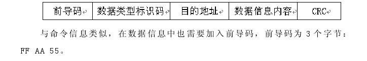
The data type identification code indicates that the information transmitted this time is data information, not command information. Its standard
The identification code is: 0XE5, which occupies one byte.
From Section 3.2.2 on the way of station coding, we can know that there is one for each station block in the city.
A specific address code indicating its unique identity, represented by 2 bytes. Such as the electronic station I address
For 0x0000, the electronic station card II address is 0x0001, and in turn, the maximum can identify 65,536 stations.
Only the stop sign with the same destination address will receive the message content.
The data information content occupies 2 bytes. Use 2 bytes of data to indicate the line number and line of the bus
Road vehicle number, in which the first 10 digits of the 2 bytes are used to compile the bus line, so that
Ensure that each city has a bus with 210=1024 lines, and the last 6 digits are used to compile the line.
The number of buses can ensure that 26=64 buses can be opened per line.
CRC is used in the communication protocol of this system
Verification, which takes up 2 bytes. When the sender sends data information, the CRC check code is placed in the transmitted signaling. After receiving the data information, the receiving end performs CRC check, compares the CRC check results, and sends a corresponding response signal according to the comparison result, so that the sending end performs corresponding processing.
2. Software process
In this bus system, since we are a self-built communication network, we must develop a suitable communication standard to establish a real-time, reliable communication network.
In addition to displaying the location information of the bus section, the electronic station card is also responsible for transmitting the traffic flow information to the next electronic stop sign and switching to the detection of the next train information, so that the relay is continued in turn.
The electronic stop sign can complete the full line communication of all the buses of the train. In order to reduce invalid transmission, we add a policy that does not send information when it is not updated. Otherwise, it sends invalid information. The workflow is shown in Figure 4.16. After the microcontroller in the electronic station card is initialized, set the timer's timing time to 10ms. Since each station stop has a uniquely identified address, only the electronic station between the addresses can establish a communication path throughout the communication link.
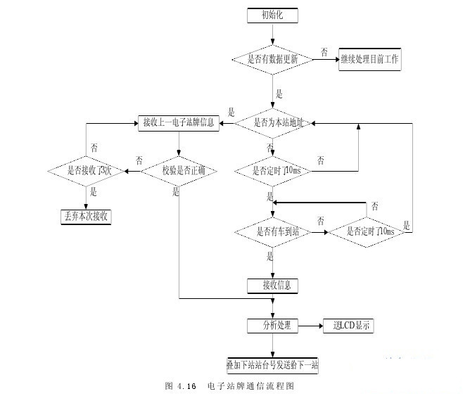
In this system, a communication link is established between the bus vehicle and the electronic station card by means of infrared transmission, and the communication link is established by the wireless module SRWF-508 between the electronic station cards. The two modes of communication link are switched every 10ms, which enables the electronic station to respond to any status request in the form of a communication link in time. Since the vehicle operation is two-way, in order to distinguish whether the information received by the station card is uplink data or downlink data,
We have the following rules: When going up, the module SRWF-508 uses an operating frequency of 425MHz; when going down, the module SRWF-508 uses an operating frequency of 433MHz. When the electronic station card detects the data information sent to it by the last electronic station card, the electronic station card is ready to receive the data information sent to it by the last electronic station card, and the electronic station card puts the received data information into the buffer. Perform CRC check, the verification result is correct, it will be sent to the LCD screen display in the station card, and the data information to be transmitted will be superimposed with the next station number, and then sent into a new data transmission package and sent to the next station; If the verification result is incorrect, the previous electronic stop sign will be requested.
Send the relevant content. If the information cannot be received correctly after 3 consecutive transmissions, the reception will be abandoned until the next communication process. When receiving the last electronic station information, the electronic station will convert the communication link every 10ms to detect whether there is a bus to send information to the station. If there is a request, the electronic station will pass the infrared module to the The bus vehicle sends back the response signal, and at the same time prepares to receive the data information. After receiving the data information, the microprocessor repackages the data information of the previous station and the local station into the buffer, displays and sends the new data packet to the next. one stop.
4.2.8 Display LCD display mode in the system
The part of the electronic station display system mainly displays the position information of the bus vehicle section. When the bus is between two stations, the block of the line and the car number sign moves back and forth between the two stations to indicate that the bus is in the two Run between stations. Figure 4.17 shows the driving route of the bus with the number n in the Wuhan Bus 724 line. For example, when the line car stops at the bus stop number 23, it will send a message to the station card. After receiving the information, the station board superimposes the information of the station and sends a new data packet to the next message. The electronic stop sign is the stop sign numbered 24 in Figure 4.17. After receiving the information, the stop sign of the number 24 is processed by the microprocessor, and the travel route map of the pre-programmed 724 line is called up, and then the travel range of the vehicle is displayed on the LCD screen of the stop sign, and the display form is displayed. A numbered block between reference numeral 23 and numeral 24 is moved back and forth between the stations to inform the passengers waiting at the station.
Liquid crystals are transparent materials with properties between liquid and solid. Under normal conditions, the liquid crystal molecules are solid, and the molecules are arranged in an orderly manner, and external light can directly pass through it. Under the action of an applied electric field, the order of the liquid crystal molecules changes, the liquid crystal molecules become liquid, and the penetration of light is affected. What is the principle of LCD display? That is, by adding voltage, the state of liquid crystal molecules changes.
Thereby changing the transmittance of the background light passing through the liquid crystal molecules, so that different images can be displayed on the liquid crystal panel. That is to say, the display effect on the LCD screen is due to the electric field applied to the display pixels, and the potential difference between the two electrodes before and after the pixel determines the pixel display state and effect.
2.LCD drive mode [44]
According to the above, the LCD display is implemented under voltage driving. The driving method is similar to the LED display, and it is divided into static driving and dynamic driving.
1 static drive mode
In a statically driven liquid crystal display device, the back electrodes of the respective pixels are connected in parallel as one pin, and the segment electrodes of the respective field pixels are respectively taken out as independent pins. If a segment is displayed, a potential field is generated between the back electrode and the segment electrode of the pixel; if a segment is not displayed, there is no potential field between them. It is easy to add a potential field at the two poles of the display pixel, but the potential field is applied for a long time, which tends to cause the liquid crystal material to age and affect the service life of the liquid crystal panel. Therefore, we must adopt the AC drive method generated by the pulse voltage situation. How can this be achieved? We can do this by applying a positive pulse sequence on the back electrode and applying a positive pulse train of equal amplitude to the back electrode on the pixel electrode to be displayed, but their phases are 180° out of phase. Then, a potential field is generated on the pixel; and an equal amplitude positive pulse sequence in phase with the back electrode is added to the pixel electrode which is not displayed, and no potential field is generated on the pixel. This is the static driving method of the liquid crystal display.
2 dynamic drive mode
The back electrodes of a group of pixels in parallel are taken together as a pin, which is called a row electrode, and the segment electrodes of a group of pixels in the longitudinal direction are connected in parallel as a pin, which is called a column electrode. This structure constitutes a matrix array, and any pixel position on the liquid crystal screen can be uniquely determined by the row and column in which it is located. The liquid crystal display controller cyclically applies a pulse to the row electrodes under the timing pulse signal, and simultaneously applies pulses to all the column electrodes of the row of pixels to enable driving of all display pixels, because the scanning cycle is short, and the cycle is continuously performed. This can make a stable image on the LCD.
We call this scan drive method a dynamic drive.
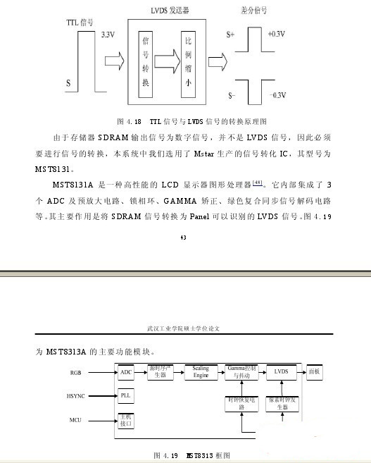
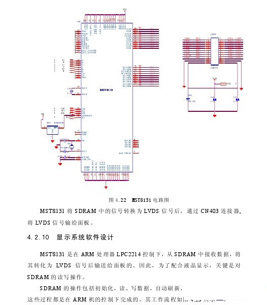
In order to save the I/O port and reduce the large-scale driving circuit, the LCD screen in this paper adopts the dynamic driving method. The ARM microprocessor converts the graphics information into bitmap format information in a specific format and stores it in the SDRAM memory. The SCALER MST8131 receives the signal from the SDRAM and converts it into an LVDS signal that the Panel can recognize.
4.2.9 Display signal processing in the system
At present, the resolution of the panel on the market is getting larger and larger, and accordingly the signal frequency is getting higher and higher. Electromagnetic interference becomes a problem that must be overcome. The LVDS signal is affected by most of the panels because of its advantages in low voltage and anti-electromagnetic interference. Manufacturer's approval, so the application of LVDS interfaces on panels is becoming more and more common.
LVDS is a differential signal technology that effectively controls electromagnetic interference. Its low voltage and low current drive outputs achieve low noise and low power consumption.
Figure 4.18 shows the conversion principle of TTL signal and LVDS signal. After the signal is converted, the TTL signal becomes two signals with the same amplitude and opposite polarity. After passing through the primary voltage proportional attenuator, the original high voltage signal can be converted into a pair of low voltage signals to reduce losses.
1 clock recovery loop
The MST8313 has an internal clock recovery loop consisting of a digital clock synthesizer and an analog circuit PLL. It is used to generate a sample clock signal to acquire analog RGB data. This loop is locked to the input line sync signal, which is used to adjust the source clock frequency (SCLK); a feedback signal is generated on the rising edge of each line sync signal input. Both the first and last line sync signals can produce a frequency of 60 MHz. Within the range of operating voltage and temperature requirements, it can be realized within 1ms.
When the panel's clock signal is different from the source clock signal (or half), there is a pixel clock used to drive the panel. It is generated by a loop that is identical to the clock recovery loop. The difference is that the source clock signal is locked to the line sync input signal and the destination clock signal is locked to the source clock signal.
2 analog to digital converter
The MST8313A integrates three analog-to-digital converters (ADCs), one for each color (R, G, B). Each ADC is an 8-bits output that converts the incoming analog RGB signal into an 8-bit digital signal, R0-R7, G0-G7, B0-B7. Signal Support: The MST8313A chip supports digitally separated signals, digital mixed signals, and analog mixed signals. All of these signals are supported without the need for additional peripheral circuitry.
3 source timing generator (STG)
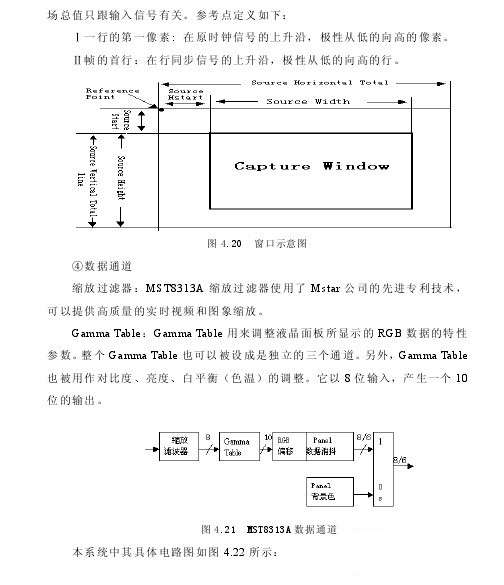
The STG module defines a graphics capture window and sends data to the data channel module. Figure
4.20 shows the definition of this port.
In the horizontal direction, it is defined in SCLKS (equivalent pixel calculation); in the vertical direction, it is defined in the line. All parameters starting with "Source" are defined in the registers of the MST8313.
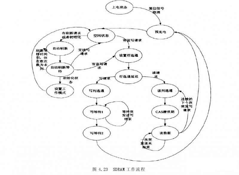
After the SDRAM drives its state to the power-on state under the action of the reset signal, the microprocessor cancels the reset signal, and the SDRAM performs a precharge, and configures the corresponding register group and control pin signals. After the pre-charging is completed, the idle state is entered. In this state, if there is a refresh request or is in the initialization phase, the automatic refresh state is entered, the corresponding signal is driven, and the refresh wait timer is started. After the automatic refresh, an automatic refresh response signal is issued, and the refresh wait state is entered. After the refresh wait timer is finished, the current refresh is ended, and then it is judged whether it is the initialization phase. If it is the initialization phase, it is necessary to enter the work mode setting state. Otherwise, it will return to the idle state when there is no read/write request operation. When there is a read/write request operation, it will go into the row strobe working mode setting state. After the row strobe, there will be one clock cycle waiting, and enter the column state working mode setting. If it is a write request at this time, the corresponding control signal is strobed, the burst enable signal is set at the same time, the operation is performed according to the set burst length, and then the write wait state is entered until the burst state ends, and then the second is entered. The write wait state is buffered, and finally returns to the precharge state; if it is a read request, the column strobe latency waits according to the programmable length after the column strobe, and then the SDRAM data appears continuously in the data port, and enters the waiting for read data state. . The read operation finally returns to the precharge state.
4.3 Summary of this chapter
This chapter discusses the hardware composition of the electronic station card, and gives the hardware circuit diagram and software design of the infrared receiving part, the wireless communication part and the display part respectively. In this chapter, the dynamic display part of the electronic station card is analyzed, and its electronic stop sign is analyzed. The actual picture is similar to the current assembly in Wuhan. The signal transmission method is different from the transmission process. In addition, we use the LCD screen to display the vehicle information. Compared with the electronic station signs currently assembled in Wuhan, the vehicle information display volume is much larger.
Wireless Video Player:
We are professional manufacture of this Wireless Video Player. It is our classic product, it is praised by our customers since it appeared on the market, it combined the DVD, TV and radio together. It has small appearance but it is a multifunction portable player.
Portable Video Player Description:
Explosion-proof glass mirror;
HD digital screen;
DVD Player, support TV and radio reception function;
Power supply: 7.4v, 4400mA;
Support video output, gold press key, MP3, TM radio, TF card plug, TV, USB interface;
Scratch-proof shell


Wireless Video Player
Wireless Video Player,Hd Video Player,Streaming Media Player,Wireless Media Player
Shenzhen New Wonderful Technology Co., Ltd. , https://www.sznewwonderful.com