Organic electroluminescent devices (OLEDs) are all-solid devices that convert electrical energy directly into light energy. They are of great concern because of their thinness, lightness, high contrast, fast response, wide viewing angle, and wide operating temperature range. It is considered to be a new generation of display devices. To truly realize its large-scale industrialization, it is necessary to improve the luminous efficiency and stability of the device and design an effective image display driving circuit. Recently, with the deepening of research, the luminous efficiency and stability of OLEDs have reached the requirements of certain applications, and its dedicated driving circuit technology is not very mature. At present, all flat panel display drivers are matrix driven, with a matrix display of X and Y electrodes. The matrix display is divided into an active matrix (AM) display and a passive matrix (PM) display according to the introduction and non-introduction of switching components in each pixel.
Starting from the TFT-OLED active matrix pixel unit circuit, this paper focuses on the voltage control type and current control type pixel unit circuit, and briefly discusses the influence of the control/drive IC on the TFT-OLED active drive circuit.
Voltage controlled pixel circuitThe voltage control type unit pixel circuit uses a data voltage as a video signal. The simplest voltage-controlled two-tube TFT unit pixel circuit is shown in Figure 1.
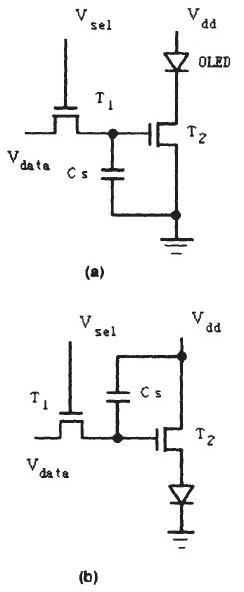
Figure 1 Two-tube TFT driver circuit
The working principle is as follows: when the scan line is selected, the switch tube T1 is turned on, the data voltage charges the storage capacitor CS through the T1 tube, and the voltage of the CS controls the drain current of the drive tube T2; when the scan line is not selected, the T1 is cut off. The charge stored on the CS continues to maintain the gate voltage of T2, and T2 remains in the on state, so the OLED is in constant current control throughout the frame period.
Wherein (a) and (b) are respectively referred to as a constant current source structure and a source follower structure, the former OLED is at the drain end of the driving tube T2, which overcomes the influence of the change of the OLED turn-on voltage on the current of the T2 tube; It's easier to implement. The shortcoming of the two-tube circuit structure is that the inconsistency of the threshold voltage of the driving tube T2 will result in uneven brightness of the display screens, and the current of the OLED and the data voltage have a nonlinear relationship, which is not conducive to the adjustment of the gray scale.
Three-tube TFT structureThe voltage control type pixel unit circuit based on the principle of the second generation current transmitter is shown in FIG. 2, the left side of the broken line can be regarded as an external driving circuit, and the right side is a unit pixel circuit.
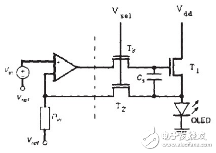
Figure 2 Pixel circuit based on the principle of the second generation current transmitter
In the control mode, T2 and T3 are turned on, and T1 and the operational amplifier constitute the second-generation current transmitter. Since the amplification factor of the operational amplifier can be made large, the threshold voltage of the T1 tube becomes insensitive to the current. Current flowing through T1:
IT1=Vin/Rin
And the source voltage of the T1 tube should be lower than the turn-on voltage of the OLED to prevent the OLED from being turned on. In the hold mode, T2 and T3 are turned off, the storage capacitor Cs maintains the gate voltage of the T1 transistor, and the current enters the OLED via T1. The amplifier is implemented by a COMS circuit, and all of the counterpart pixels can share an operational amplifier.
The simulation results show that although the T3 tube has charge injection and clock feed leakage effect, the OLED current is slightly smaller than the control current. When the nominal current of the OLED is 1μA and the threshold voltage drift exceeds 5V, the relative error of the control current and OLED current is -0.18. %, 5.2%, successfully compensated for the spatial heterogeneity and instability of the TFT.
Four-tube TFT structureDawson et al. first proposed a unit pixel circuit of a four-tube TFT structure, which compares the data signal with the drive tube by auto-zeroing to eliminate the offset of the TFT gate voltage and apply a prioritized zero signal before the data signal ( VAZB), the charge accumulated by the parasitic capacitance is released, solves the problem of threshold voltage variation, and does not depend on the opening and charging time of the OLED. A drawback of this type of circuit is that when the channel length becomes shorter, uneven illumination will occur.
GohJC et al. proposed a sub-threshold current compensation threshold voltage change voltage control type circuit, adding a compensation phase to the driving timing to operate the driving tube in the sub-threshold region. At this time, the gate-source voltage of the driving transistor, that is, the threshold voltage Vth is stored in A storage capacitor that compensates for the drift of the TFT threshold voltage during the data input phase. They also proposed a voltage-controlled drive circuit that utilizes the discharge-compensated threshold voltage variation. Unlike the former, the circuit uses the discharge method to cause the drive tube to enter the sub-threshold region to obtain a superposition of the data voltage and the threshold voltage, thereby effectively compensating Threshold voltage change.
In addition to effectively compensating for threshold voltage variations, the voltage-controlled drive circuit has the advantage of having a fast response characteristic. Since the voltage is directly applied to both ends of the storage capacitor CS, the charging current initially has an instantaneous large current to charge the capacitor. Greatly reduced charging time.
Solar mobile Power Bank is a new type of power source that converts solar energy into electric energy and stores it in a battery, and at the same time has a mobile nature. The storage battery can be any form of power storage device, which is generally composed of three parts: solar photovoltaic cell, storage battery, and voltage regulating element.
With the energy crisis and the deteriorating environmental problems caused by petrochemical fuels, people are paying more and more attention, and the current digital products are becoming more and more popular. Solar mobile power is developed under this background.
solar power bank, power bank solar, solar power bank waterproof, solar power bank 30000mah, solar charger power bank, portable solar power bank
Reteck Electronic Co., Ltd. , https://www.reteck.com