At present, research on WSN (Wireless Sensor Network) mainly focuses on protocol stack, positioning algorithm, energy management and architecture design, while research on wireless sensor network operating system is relatively rare, especially for its underlying platform. There are fewer studies, so there is a very broad space for research on the underlying platform of wireless sensor network operating systems. This paper introduces the STMicroelectronics STM32 series MCU and TI's CC2520 wireless module. It mainly describes the construction of the underlying platform of the operating system and the implementation of hardware drivers. The underlying hardware abstraction layer of this paper is for the CC2520 wireless RF module, including platform construction, related registers, and peripheral interfaces. The hardware driver is mainly designed to complete the hardware driver required for wireless communication. This mainly includes: the interrupt mechanism of the corresponding asynchronous event; the USART driver for PC communication; the SPI driver for connecting MCU and CC2520; the timer for completing the timeout timer, etc. . The effective composition of these modules can constitute a complete wireless sensor network minimum communication system, complete data transfer between nodes, data processing, and positioning and navigation tasks.
The STM32 series MCUs use the CortexM3 core of the ARM V7 architecture. The CC2520 is the second generation ZigBee/IEEE 802.15.4 transceiver.
1 Underlying platform research
There are many low-level hardware modules in the hardware abstraction layer. This section only briefly introduces the underlying module design related to wireless sensor networks.
1.1 Timer
The STM32 series of CPUs can provide eight timers, of which TIM1 and TIM8 are advanced timers that can be used for a variety of purposes, including measuring the pulse length of an input signal (input capture) or generating an output waveform (output comparison), etc. Provided by APB2. TIM2~TIM7 are ordinary timers, and the clock is arched by APB1. Figure 1 shows the portion of the timer in the STM32 clock tree.
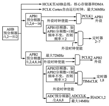
Figure 1 Clock tree for timers in STM32
As can be seen from Figure 1, the clock frequency generated from the clock source set by the system is input to the AHB prescaler for frequency division processing, and then different clocks are provided to different modules through the APB1 prescaler and the APB2 prescaler. frequency. The timer 2 is taken as an example below. When the input frequency of the AHB prescaler is 72 MHz, since the maximum frequency supported by APB1 is 36 MHz, the APB1 prescaler must be set to be greater than or equal to 2. If it is set to 2, it is in the APB1 multiplier. The frequency is set to 72 MHz (when the APB1 frequency division number = 1, the APB1 frequency multiplier doubling coefficient is 1, when the APB1 frequency division number is 1), the APB1 frequency multiplier doubling coefficient is 2), so the final The frequency for timers 2 to 7 is 72 MHz. Therefore, it is only necessary to set the values ​​of the APB1 prescaler and the APB1 multiplier to provide timers of different frequencies. The timer triggers the timer interrupt by counting overflow. Therefore, to use the timer, the timer interrupt must be configured first.
1.2 Interruption
The interrupt configuration steps for the STM32 series MCU are as follows:
1 System initialization: If the system clock is initialized, use the SystemInit() function that comes with the firmware template. This function adjusts the main frequency to 72 MHz by default.
2 GPIO configuration: Configure the pin that triggers the CPU interrupt. Be sure to turn on the GPIO clock and AFIO clock of the corresponding pin. Configure the frequency and input mode of the pin, typically in floating input mode.
3 EXTI Configuration: First indicate which pin is used in the current system as the pin that triggers the external interrupt, then clear the interrupt flag, configure the interrupt request and trigger mode (rising edge trigger or falling edge trigger).
4 NVIC configuration: Mainly configure the channel corresponding to the interrupt, and set the priority level. Finally, you need to enable the channel.
5 Write the interrupt service program: The interrupt service program is the program that actually runs when the interrupt occurs. It interrupts the running program and processes the corresponding interrupt event accordingly. Since the interrupt program interrupts the running of the existing program and needs to respond quickly to the interrupt event, it should be as short as possible, and the parameters cannot be passed, and there is no return value.
1.3 USART
The USART module is generally divided into three major parts: a data transmitter, a data receiver, and a clock generator. All modules share control registers. The clock generator consists of a baud rate generator and a synchronous logic circuit.
The data transmitter portion is composed of a write buffer register (USART_DR), a check digit generator, a serial shift register, and a control logic circuit. Multi-frame data can be sent continuously and quickly using the write buffer register.
The data receiver is the most complex part of the USART module, the most important being the data receiving unit and the clock. The data receiving unit is used as a reception of asynchronous data. The data receiver also includes a shift register, control logic, a check digit checker, and a receive buffer. The data receiver supports the same frame structure as the data transmitter, while supporting the detection of data overflow, framing errors and check errors.
The wireless node can communicate with the PC via the USART. This article only implements a simple USART function. The serial port needs to be initialized before use. It mainly sets the word length, baud rate, parity, transmission mode, data digits, flow control, open serial port clock, and configure serial port transmit and receive pins.
With the input/output function of the serial port, you can rewrite the library function printf yourself, which is convenient for debugging and observing the running status of the node, allowing the output of the node terminal to be redirected to the PC, and then displaying the data information sent by the node through the serial port tool on the PC. Thereby analyzing the operation of the terminal. The specific function design is: if the node outputs the string data, the serial output string function is directly called, and the string data is sent to the PC through the serial port; if the number is output, the number is first converted into a string according to the specified display hex. And then processed as an output string. You can override the itoa() function to save the entered number to a string in arbitrary hexadecimal.
1.4 SPI
The SPI has three registers: a control register (SPI_CR), a status register (SPI_SR), and a data register (SPI_DR). The SPI interface consists of four types of signals: MOSI - slave data input, master data output; MISO - slave data output, master data input; SCLK - clock signal, generated by the master; NSS - slave select The enable signal is controlled by the master device, and some chip manufacturers will mark it as CS (Chip Select).
Since the wireless module CC2520 must communicate with the MCU through the SPI interface, the SPI interface must be implemented to control the CC2520 to receive and transmit data. The processing of the SPI interface is very similar to that of the USART interface. This article only implements a simple SPI function. The SPI must be initialized before use. The main tasks include setting the master-slave mode, baud rate, number of data bits, data frame format, configuring the input/output pins, and the phase and polarity of the clock signal.
1.5 CC2520 driver
The MCU controls the CC2520 to start, shut down, send and receive data, etc. through the SPI interface. The SPI interface consists of four pins, SI, SO, CSn, and SCLK. In the communication process between MCU and CC2520, CC2520 is the SPI interface slave device, receives the clock signal and chip select signal from the MCU, and performs operations such as sending data and receiving data under the control of the MCU; STM32 is the interface master device and can pass The SPI interface accesses the internal memory and registers of the CC2520. The CC2520 uses four pins, FIFO, FIFOP, SFD, and CCA, to indicate the operating state. The MCU can read the data of these pins to get the status of the CC2520 transceiver data. The SFD signal indicates that the frame start signal has just been received or has just been transmitted; the FIFO signal indicates that one or more bytes are in the receive buffer; the FIFOP signal indicates that the number of bytes in the receive buffer exceeds the set threshold or at least one frame is received. Data; the CCA signal indicates that the channel is idle.
CC2520 probably work flow: First, preparation work. The upper layer application uses the halRfInit() function to perform some initialization of the CC2520. For example, reset the CC2520 and turn off the voltage regulator. The CC2520 data sheet requires a delay of 1100 μs. After the delay is completed, turn on the voltage regulator, delay 200 μs, then enable CC2520. After completion, apply for SPI resources and initialize. Turn on the oscillator, then configure the default values ​​of some registers in CC2520 through the SPI interface, such as the values ​​of TXPOWER, CCACTRL0, MAMCTRL0, MAMCTRL1 and other registers. The MCU and CC2520 connected pins are then initially configured, such as RSTN, VREN, and CSN configured as output modes, with FIFO, FIFOP, CCA, and SFD configured as input modes.
The upper layer application uses the basicRfInit() function to complete the setting of the channel, short address, and network ID, and configures the receive interrupt processing function to process the received data when the data is generated.
When the application executes the send command, the data is encapsulated from the upper layer according to the protocol stack, and finally the data is handed over to the basicRfSendPacket() function. The specific sending process is shown in Figure 2.
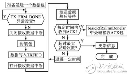
Figure 2 CC2520 sending data flow chart
The format of the encapsulation in the figure is in accordance with the protocol requirements, and the content mainly includes data length, frame control domain (FCF), destination address, source address, destination network ID, source network ID, transmission data, and CRC (Cyclic Redundancy Check) check code. When the hardware CRC check is used, the user does not need to calculate the CRC check code, nor does it need to write the CRC check data into the TXFIFO (CC2520 transmit buffer). There is a special register to store the CRC check data, which is verified and sent by the hardware. . When using the software CRC check, the user needs to calculate the CRC check data by himself and fill it in the last two bytes of the frame and write it to the TXFIFO along with other data in the frame.
After the package is completed, the data is written into the TXFIFO. Note that the CC2520 send buffer is 128 bytes, which cannot exceed this range. Otherwise, the TX_OVERFLOW exception will be raised. Then, after the receiving data is interrupted, the sending command can be called to send data. Here, the sending process can be completely controlled. For example, in the process of transmitting data, the rising edge signal of the SFD pin can be captured to accurately time the transmission. After the data is sent, the receiver waits for the ACK to reply. If the ACK is not received within the specified time, it determines whether the number of retransmissions exceeds the maximum number of retransmissions. If not, the packet is retransmitted according to a certain policy for a period of time. The maximum number of retransmissions discards the packet and sets the transmission failure flag for the upper layer program reference. If the ACK is received within the specified time, the RX_FRM_DONE interrupt will be triggered, and the basicRfRxFrmDoneIsr() will be called to receive the data interrupt handler to analyze the received ACK packet. If it is a correct reply to the packet just sent, it indicates that the transmission was successful and updated. Corresponding information, such as sending sequence number plus 1, updating the sending status, clearing TX_FRM_DONE exception, etc.
The receiving process is similar to the sending process. The specific receiving process is shown in Figure 3.
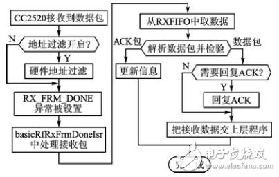
Figure 3 CC2520 receiving data flow chart
1, Quick Measuring: Medical Grade Instant infrared Thermometer is suitable for kids, infants and adults, measurement speed is 1S, faster than conventional thermometers. This Infrared Thermometer adopts refined superior microchip and high sensitive sensor, make infrared thermometer high accurate and rapid no contact scan for people, objects and rooms
2, High Accurate Test Result: The infrared thermometer is Hospital Grade, measurement accuracy is ±0.2℃. Typical application in your home, clinic or workplace, bus, shops, schools, subway, library etc
3, Three measurement mode: The thermometer enables you to measure human, room or object temperature instantly with the press of a mode button. Perfect suits for parents, teachers, nurses, who want to keep a close eye on the body temperature of babies, children and patients.
4, Easy to Use: quiet scan temperature mode allows you to take instant scans of infants and children without a beeping noise. Celsius and Fahrenheit are easily and instantly switchable with an intuitive button.
5, Indicative Color: Temperature will be displayed on the LCD screen with clinically proven accuracy you can rely on. Three color backlight, green, orange, red, even easily readable in the dark.
5, FDA, CE, ISO certificates
Non Contact Thermometer, Infrared Thermometer,Non contact Baby Thermometer,COVID19
Axiswell Technology Co., Ltd , https://www.medhealthycare.com