I. Project Overview
1.1 Project Summary
The system uses FPGA as the control core, and is composed of MOSFET full-bridge inverter circuit and its IR2110 drive, SPWM (sinusoidal pulse width modulation) wave generation, voltage and current detection, phase frequency tracking and other modules. The SPWM wave is generated by comparing a sine wave of a triangular wave generated by software inside the FPGA with a digital comparator. The modulation ratio is adjusted by changing the amplitude of the sine wave, and the duty ratio of the SPWM wave is adjusted to adjust the voltage to achieve maximum power. The MPPT algorithm is used to maximize the power tracking of the system. This system also implements undervoltage and overcurrent protection of the system, and controls in the same frequency in phase.
1.2 Project Background / Motivation
With the increasing consumption of energy and the diminishing reduction of traditional energy sources, as well as the increasing number of related problems caused by the use of traditional energy sources, such as environmental pollution, greenhouse effect, etc., the demand for new energy sources is increasing. The bigger. Photovoltaic grid-connected is the development trend of solar energy utilization, and photovoltaic power generation system will be mainly used for peaking power station and rooftop photovoltaic system. In the photovoltaic grid-connected system, the grid-connected inverter is the core part. The DC-AC inverter link mainly makes the output current and the grid voltage in phase, and just obtains the unit power factor.
Motivation of the topic: At present, the power industry as an infrastructure is making efforts to use solar energy to inject new vitality and vitality into the development of electricity. Photovoltaic grid-connected power generation has become the trend of the times and the key technology that restricts solar energy applications. This design mainly studies some technologies in optical grid-connected power generation. This design mainly realizes the conversion of analog photovoltaic power source from DC to single-phase AC power. The function, with maximum power point tracking and frequency phase tracking, adds related protection and display functions. Moreover, the solar photovoltaic power generation market has received the attention of governments and the state has a large degree of support. On July 30, 2011, China's first public security fire station using solar power generation was put into use, and photovoltaic power generation has broad prospects.
Second, the demand analysis
2.1 Functional requirements
Design and manufacture a photovoltaic grid-connected power generation simulation device, and its structural block diagram is shown in Figure 1. Use DC power supply US and resistor RS to simulate photovoltaic cells, US=60V, RS=30Ω~36Ω; uREF is the sinusoidal reference signal of analog grid voltage, its peak-to-peak value is 2V, frequency fREF is 45Hz~55Hz; T is power frequency Isolation transformer, the ratio is n2: n1 = 2: 1, n3: n1 = 1: 10, uF as the feedback signal of the output current; load resistance RL = 30 Ω ~ 36 Ω.
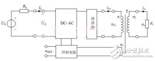
Figure 1 Block diagram of grid-connected power generation simulation device
(1) With maximum power point tracking (MPPT) function: When RS and RL change within a given range, the absolute value of relative deviation is not more than 1%.
(2) With frequency tracking function: When fREF changes within a given range, the frequency of uF is fF=fREF, and the absolute value of relative deviation is not more than 1%.
(3) Realize phase tracking function: When fREF changes within a given range and adds non-resistive load, uF and uREF can be guaranteed to be in phase, and the absolute value of phase deviation is ≤5°.
2.2 Performance standards
(1) When RS = RL = 30 Ω, the efficiency of the DC-AC converter is ≥ 80%.
(2) When RS = RL = 30 Ω, the distortion of the output voltage uo THD ≤ 1%.
(3) With input undervoltage protection, the operating voltage Ud(th) = (25 ± 0.5)V.
(4) It has an output overcurrent protection function, and the operating current Io(th)=(1.5±0.2)A.
(5) After the overcurrent and undervoltage faults are eliminated, the device can automatically return to the normal state.
(6) When the load temperature is too high, the system stops working.
Third, the program design
3.1 System function realization principle
1. Maximum power tracking scheme
Adopt the classic MPPT algorithm, continuously sample the output voltage and current of the photovoltaic power grid, and find the point where P=U*I is the largest, that is, the maximum power point. This method variation step is determined by the rate of voltage change at the output of the simulated photovoltaic cell, which can quickly approach the maximum power point.
2. DC-AC circuit scheme
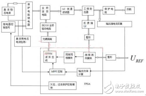
We use FPGA to generate SPWM wave signal to drive half-bridge or full-bridge DC-AC inverter, and obtain the inverter signal after output LC filtering. The generation of SPWM waves in this scheme is implemented by software. The inverter circuit of DC-AC is built by discrete components, and the circuit is built by high-speed power switch IRF540N and MOS tube driver chip IR2110. The on/off voltage of the MOS transistor is adjusted by adjusting the modulation ratio, thereby adjusting the magnitude of the inverter voltage.
3. Implementation of co-channel in-phase control scheme
The edge trigger method and the digital feedback adjustment method are used for adjustment. After the input reference signal and the feedback signal are respectively shaped by the comparator, the rising edge is detected. This operation is realized by hardware to obtain the difference between the frequency and the phase, and the phase of the input signal is phased by the digital feedback inside the FPGA. Adjustments, these operations are implemented by software.
4. Undervoltage, overcurrent, over temperature protection circuit
By detecting the input voltage Ud, the input current Id and the output current Io are converted into digital signals by the ADC0809 and fed back to the FPGA control system. The FPGA controls the relay to perform undervoltage and overcurrent protection. The load temperature is measured by a temperature sensor, and the control relay is turned off when the temperature is too high.
System hardware block diagram
5. Single-phase full-bridge inverter circuit and its driving circuit
The IR2110 is a half-bridge driver chip, which only needs to be connected to the bootstrap capacitor. The internal bootstrap circuit can be used to drive the bridge. For the full-bridge circuit, only two IR2110s can be driven to drive the respective half bridges.
6. Measurement of voltage and current
The input current is measured by measuring the voltage across the small resistor connected to the loop, and then amplified by the AD620 100 times, and then A/D conversion is performed to let the FPGA calculate the current detected at that time and display it;
7. The output current Io is AC. It is amplified by 100 times as well as the current method of the input terminal, and then converted to DC voltage by AD637 and then calculated and displayed in (2).
3.2 Hardware Resource Configuration
The amplifier uses the AD620, the RMS conversion uses the AD637, the A/D conversion uses the ADC0809, the minimum system uses the FPGA, the driver chip uses the IR2110, the MOS transistor uses the IR540, and the temperature sensor uses the temperature sensor in the STEVAL-MKI062V2 development kit from ST. And some components
3.3 system software architecture
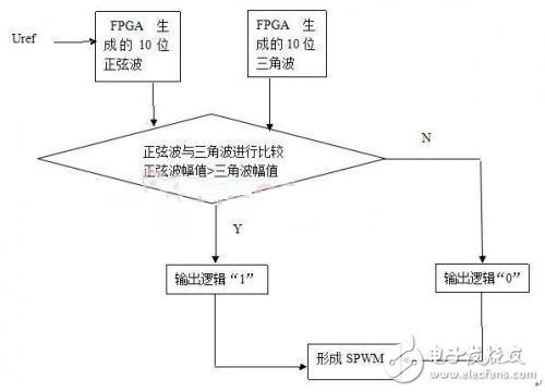
Triangle wave generation: The counter is increased from 0000000000 to 1111111111, and then reduced from 1111111111 to 0000000000, then a 10-bit triangular wave can be obtained.
Sine wave generation: Use MATLAB to generate a ten-bit mif file, then generate 1024 addresses from these 1024 points, store the address in ROM, and read the sampled data to get the desired sine wave.
SPWM wave generation structure block diagram:
Software architecture diagram
The SPWM wave is compared with a sine wave by a triangular wave. When the amplitude of the sine wave is greater than the amplitude of the triangular wave, the output is high, and vice versa.
3.4 System Software Process
The FPGA first converts these values ​​by detecting the input voltage and current read from the ADC0809, and the output current. For example, the current value is calculated, and then compares the undervoltage and overcurrent, if undervoltage or overcurrent. The control relay is disconnected and detected again after 0.5s. If there is no undervoltage or overcurrent, the maximum power tracking is performed directly, and then the input voltage and current, output current and input power are displayed on the LCD.
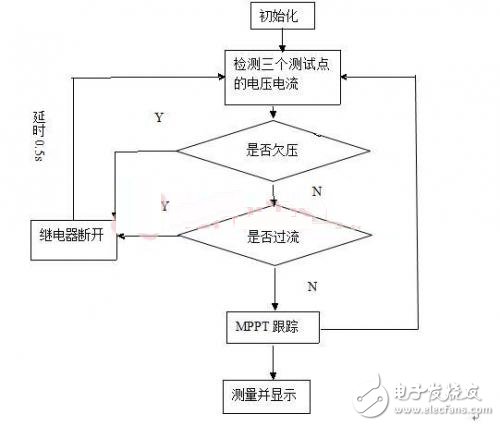
Program flow chart
Linear Stepper Motor,Linear Actuator Motor,Nema Stepper Motor,Linear Drive Motor
Changzhou Sherry International Trading Co., Ltd. , https://www.sherry-motor.com