The circuit in this design consists of a mixed-signal microcontroller, a USBUART (Universal Asynchronous Receiver/Transmitter), and a novel adaptive analog sensor input circuit. This circuit can connect multiple types of sensors to the two analog input channels of the design, control these devices on a USB host, and read the measurement data. The USB connection provides power to the circuit. The device can be controlled with simple commands on the computer; even with the terminal software, the measurement can be done. The 8051 core has free tools for programming, such as IDE (Integrated Development Environment), debugger, and C compiler.
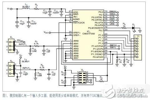
The design uses a $8 8051 architecture microcontroller, a PGA (programmable gain amplifier), and a 24-bit sigma-delta ADC (Figures 1, 2, and 3). Microcontroller IC1 has an input multiplexer that can be used in differential mode or single-ended mode. It also has two DAC outputs that can provide five unspecified digital I/O pins (Figure 1). One output pin drives the D1 controlled by the program. The other digital pins are used to configure two analog inputs. In addition, the microcontroller's reference output can also be sent to an analog input port. The remaining four digital pins are connected to the USB UART chip.
Schematic
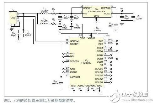
The 3.3V linear regulator IC2 powers the microcontroller (Figure 2). From the USB port through the magnetic beads and filters, you can directly power the USB chip IC1. This chip is a common and reliable USBUART chip that communicates with computers that use any operating system. The op amp IC4 acts as a buffer for the microcontroller's reference output (Figure 3).

Op amp IC schematic
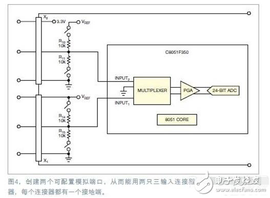
With two three-input connectors, many types of sensors can be connected to two configurable analog ports, each with a ground (Figure 4). One ground provides a 3.3V supply and the other outputs a buffered reference that is rated at 2.5V. The middle pins of the two connectors are connected to the microcontroller's analog input multiplexer. This way, you can measure two single-ended voltages or use two connectors as differential inputs. Both inputs have pull-up and pull-down resistors R10, R11, R14 and R15 that are independently switched.
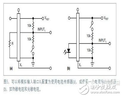
The analog input architecture is capable of directly connecting multiple types of sensors. For example, a thermistor or photoresistor can be connected between the ground and the input, and the pull-up resistor can be connected to form a voltage divider; the on-chip ADC can directly digitize the output of this voltage divider (Figure 5). . This approach also uses a ratiometric approach, meaning that the ADC uses the same voltage reference as the voltage divider drive voltage. The current output sensor can also be connected like a photodiode, ie directly connected between the ground and the input. Switch to the pull-down resistor so that the photocurrent can generate a voltage.
Ground terminal diagram
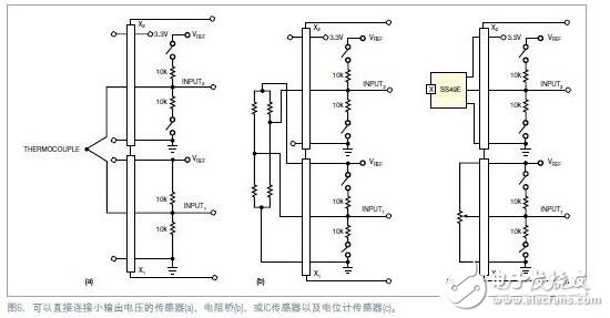
The high resolution ADC and PGA can be connected directly to the thermocouple (Figure 6). The desired bias point can be achieved by switching the pull-up and pull-down resistors on one channel. By turning off all built-in resistors, you can use directly connected bridge sensors (such as load cells and pressure sensors). In these cases, the ADC should be operated in differential mode. Making all open switches is also suitable for applications with potentiometer inputs or IC sensors, such as the SS49E Hall-effect magnetic field sensor.
Connection diagram
Source impedance, signal range, filtering, and noise picking issues should be considered when using directly connected sensors. You may need to add additional buffer amplifiers, or more precise voltage references. This configuration is made possible with a 3.3V supply of voltage reference and analog port. Alternatively, the DAC output in connector J 1 can be used to adjust the value or provide an arbitrary voltage to the sensor. Note that J1 also has five digital I/O pins (Figure 1).
Circuit board
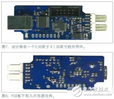
The design is housed in a 2.36" & TImes; 1.38" housing (Figure 7) with several passive components under the PCB (Figure 8). Provides details that can be downloaded to the entire design, as well as CAD/CAM files, bill of materials, and software.
Tv Guard,Universal Tv Guard Surge Protector,Tv Guard Surge Protector,13Amps Tv Guard Surge Protector
Yuyao Huijun Electrical Appliance Co., Ltd. , https://www.yyhjdq.com