A design method of radar receiver system based on ADS
introduction
Monolithic, modular, and modernization are the development trends of modern receiver technology, including receivers in the field of communications, radar, and other related fields. However, as the research and development cycle of various new devices becomes shorter and shorter, the update of radar receivers is required to be faster and faster, which puts new and higher requirements on the design of receiver systems. In the traditional receiver system design, the design and simulation of digital circuits are very mature, and its RTL and system-level simulation tools have appeared in large numbers; but in terms of analog circuit design, such high-level simulation and synthesis tools are still relatively backward. In the past, the analog front-end design was basically relied on the system engineer ’s many years of experience or even intuition. There was no optimization and distribution at all [1], which severely constrained the system development cycle.
With the increasing complexity of circuit structures and the increase in operating frequency, EDA software has become an indispensable and important tool in the process of circuit and system design. The speed, accuracy and convenience of the simulation analysis method provided by the EDA software are very important. In addition, the connection between the software and other EDA software and measuring instruments is also one of the functions that must be possessed by the current huge design process. The ADS software launched by Agilent has become one of the most used software in universities and research institutes in China with its powerful functions. The system design method in this paper is based on ADS software for simulation analysis.
System design method
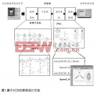
The system design method proposed in this article starts with the system as a whole, allocates the overall indicators to different modules through budget analysis, and after obtaining the specific indicators of each module, the specific design of each module can be carried out, and then verify its feasibility, thereby greatly shortening the design time, Improve the reliability of the design and avoid duplication of work and waste of resources. This method eliminates the blindness of previous design methods, and will use quantitative optimization methods to design from top to bottom, as shown in Figure 1. The traditional design is generally bottom-up, first designing each unit module, and then combining them into the whole system. On the one hand, it may fail to meet the overall requirements; on the other hand, in order to meet the overall index, the difficulty of unit module design is increased; in addition, for different system requirements and standards, it must also be redesigned, laborious and time-consuming. Using a top-down design method completely avoids these problems.
Optimized selection of system structure
Today's radar receiver systems must meet stringent specifications in various signal links while meeting various standards. According to the preset performance indicators of the radar receiver, the system structure is optimized and selected. First, the performance of various receiver structures is simulated and analyzed to obtain rough performance limit boundaries; at the same time, the system optimization ideal behavior model is established according to the key performance indicators. And use a large number of measured product behavior models to modify. For example, a link budget simulation must be performed on the system to estimate whether the overall performance meets the receiver system requirements, and at the same time as a basis for device selection.
The conventional structure of the radar receiver is shown in Figure 2.
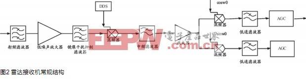
Based on the traditional receiver structure design, the receiver structure can be classified from the aspect of spectrum utilization [2] [3], and only the receiver structure with medium spectrum utilization is briefly introduced here.
In this structure, the number of unused frequency bands is approximately equal to that occupied by the system, so the RF front-end should support simultaneous sensing activities on several frequency bands simultaneously. From a circuit point of view, the number of receiver components has greatly increased. From practical considerations, the number of parallel processing channels should be controlled at 4 or 5 channels. At this time, high power is required to accurately control multiple local oscillator signals, and they need to work on a fixed frequency, so the requirements are correspondingly very broad. In order to achieve parallel consistency, the available frequency must be sufficient, and the channel calibration algorithm can be used to calibrate the channel after the ADC [4]. Therefore, the baseband port of the parallel channel increases the bandwidth, which requires an A / D converter with a higher rate and resolution than in low-frequency spectrum utilization.
In summary, different system structures have different performance index limits and integration levels, and the index limits and integration levels change as the process improves. Therefore, when optimizing system structure selection, we must also consider the impact of future process, power supply voltage, and circuit structure evolution on the optimization model.
The system model of the receiver structure with medium spectrum utilization is shown in Figure 3.
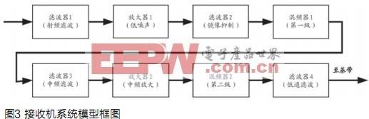
The system performance vector thus obtained is:
![]()
Where A1 represents the structure performance vector of the receiver with medium spectrum utilization, f1, f2, f3, and f4 represent the performance function of each filter, a1, a2 represent the performance function of each amplifier, m1, m2 represent the performance function of each mixer .
Through a similar method, the performance vectors A2 and A3 of the receiver structure with low spectrum utilization and high spectrum utilization can be obtained, respectively, and finally through the optimization function:
![]()
The optimal receiver system structure is obtained.
Through this simulation, you will see the distribution of the total system gain in each part of the system. Budget gain simulation can be performed in both harmonic balance analysis and AC analysis, but if it is performed in AC simulation, the mixer cannot be transistor-level. The behavior-level simulation is performed here, and the nonlinear characteristics of the mixer are known, so AC analysis is needed for simulation [4] [5].
The simulation will be carried out under the two conditions of maximum and minimum total gain of the receiver in order to obtain more comprehensive analysis results. When the VGA gain is at its maximum, the power level of the signal source is the receiver's sensitivity of -113dBm (the loss of the antenna duplexer has been considered); conversely, when the gain of the VGA is at its minimum, the signal source should be input to the receiver. The maximum power received. These parameter changes must be set in VAR.
You can set the budget path and establish the budget equation on the basis of the original block diagram. The author's two simulation results, as shown in Figures 4 (a) and 4 (b), can clearly see the receiver's maximum and minimum VGA gain The distribution of the overall machine gain.

It can also be seen from Figure 4 that the receiver front-end generally requires the addition of AGC in order to dynamically adjust the input power of the input signal to match it to the ADC.
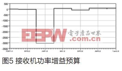
Figure 5 shows the receiver power gain budget, from which you can see the distribution of power gain on each device.
Optimized selection of RF modules
In the optimization selection of the system structure, the optimal system structure has been obtained. The system performance indicators cannot be directly applied to structural planning and module design. These indicators need to be converted into parameters that directly reflect the performance of the RF module, such as noise figure, linearity, stability, etc., so specific performance parameters can be assigned to each RF Module.
Radio frequency modules can generally be divided into amplification, filtering, mixing and other modules. Taking an amplifier as an example, its actual behavior model must also consider various nonlinear factors.
â— Noise. It can be considered as random interference that is not related to useful signals. There are mainly three types of thermal noise, shot noise and flicker noise. The noise figure of the receiver mainly depends on its front-end circuit. If there is no high-frequency amplifier, it is mainly determined by the mixing circuit.
â— Linearity. The indexes used to measure linearity mainly include third-order intermodulation, second-order intermodulation, and 1dB compression point.
â— Stability. Because the transistors have internal feedback, when the feedback reaches a certain level, it will cause the stability of the amplifier to deteriorate and cause self-excitation.
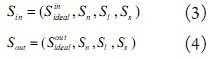
These nonlinear factors are not isolated, but superimposed with the input signal to form the input and output of the system. With Sideal, Sn, Sl, and Ss representing the ideal signal, noise, linearity, and stability of the module, the input and output signals can be expressed as
So you can get the behavior model of the actual device, and analyze its performance in combination with ADS simulation
Device selection
Only some typical devices such as RF filters and low noise amplifiers are simulated and analyzed here.
filter
Because the weak RF signal received by the antenna is directly filtered, the insertion loss and in-band fluctuation of the RF filter are required to be as small as possible. In order to meet the system performance requirements and improve the dynamic range of the receiver device, several sets of filters are usually needed to reduce the number and amplitude of interfering signals and the noise entering the receiver. At the same time, in order to cover the entire frequency band, the use of electrically tuned filters is an inevitable trend. The electric tuning filter is to change the frequency response of the network by changing the variable capacitance in the filter network. Use the voltage to change the capacity of the variable capacitor to achieve the required frequency response. In this design, each frequency band can be covered with an electrically tuned filter.
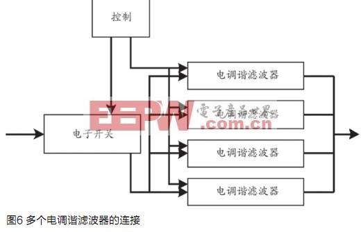
The connection of multiple electric tuning filters is shown in Figure 6. The input signal is the radio frequency signal received by the antenna, and the output signal is the signal selected by the electric tuning filter, which can satisfy the filter Device). Therefore, using the electronic switch and the control port of the signal processor, the filter can be placed in any band of interest in the band.
Low noise amplifier
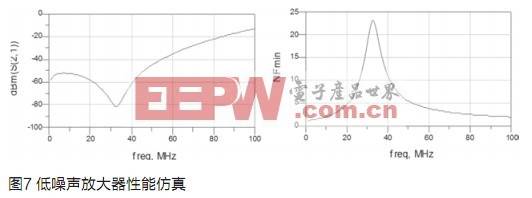
According to the required sensitivity, band-pass filter insertion loss and ADC input level requirements, design amplifier gain and matching issues. When constructing the circuit, pay special attention to the choice of power supply bypass, parasitic capacitance and peripheral components to give full play to the performance of low-noise amplifiers. This article can use ADS software to design a low-noise amplifier according to the parameter requirements, and optimize and simulate its parameters to obtain the simulation results shown in Figure 7. It can be seen from the results that this low noise amplifier basically meets the design requirements and can be used in system design. Then the circuit layout can be drawn according to the results of the software design and processed into a circuit board. Finally, debug the processed circuit to meet the design requirements. This work will be completed in the future.
Combining the above design method with the traditional baseband equivalent system optimization method, a top-down design process that can comprehensively evaluate the system structural performance is formed.
Conclusion
In this paper, based on the conventional receiver design method, using ADS software, an efficient system design method is proposed. After verification, the development cycle of the radar receiver system has been greatly shortened, and it has been gradually applied in the project group of the author.
The main control unit of the equipment is PLC and the HMI (Human Machine Interface) is 7" LCD colorful touch screen. The equipment has varieties of operating modes, and can automatically record and save working status.The complete set of equipment is easy to operate, reliable in working, complete in protection and high in automation.
It has the features of high reliability, high pulse symmetry, strong anti-interference ability, quick reaction, as well as the advantages of no heat-generating, constant current, energy-saving which is compared with the discharge with the electrical resistance.
Agv Battery Charger And Discharger
Battery Charger Discharger,Charging And Discharging Of Battery,Intelligent Battery Charger And Discharger,Agv Battery Charger And Discharger
Xinxiang Taihang Jiaxin Electric Tech Co., Ltd , https://www.chargers.be