1 Introduction
With the continuous development of electronic systems, the demand for data transmission between chips and boards is also increasing. The traditional single-ended parallel data transmission mode has long been unable to meet the requirements of high-bandwidth applications. The release of new serial specifications such as USB 3.0, SATA 3.0, PCI-E 2.0 and the introduction of higher-speed serial-parallel / parallel-serial conversion unit (SERDES) chips have caused the industry's unlimited expectations for high-speed differential serial data transmission. In order to solve the huge data throughput requirements brought by multi-antenna (MIMO) signal processing in the next-generation wireless communication base station, this paper gives a realization based on the Virtex-5 FPGA GTP unit in an advanced telecommunications computing architecture (ATCA) chassis The design scheme of 3.125Gbps serial transmission for a single pair of differential lines.
2 Transmission system design
The composition structure of the transmission system is shown in Figure 1, which is mainly composed of two ATCA boards and an ATCA chassis backplane. Two FPGAs are placed on each of the two ATCA boards as the two endpoints of the serial link, and two pairs of differential lines are used to connect the two FPGAs to form a bidirectional serial communication link of 3.125Gbps each. In order to verify the long-distance transmission capability of the system, two boards were placed in physical slot 1 and physical slot 14 of the 14-slot ATCA chassis. At this time, the total transmission distance was approximately 40 inches.
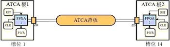
Figure 1 The overall structure of the high-speed serial transmission system
Because the backplane performance of the existing ATCA chassis cannot be changed, the main design of this article focuses on the design of the ATCA single board, mainly the laminated design of the single board, the power supply design of the FPGA as the transmission endpoint, and the reference clock design of serial transmission And the parameter adjustment of the GTP transceiver unit inside the FPGA.
2.1 Laminated design
The stacked design is the basis of other designs. This system mainly considers two aspects when designing the stacked structure: First, let all GTP transceiver differential lines be distributed on the stripline signal layer instead of the unilaterally coupled microstrip line Signal layer. Although the stripline has a larger loss than the microstrip line, the impedance of the stripline is more controllable, and the coupling with the AC ground plane is better, which is conducive to the return of high-speed signals; the second is to reduce the power supply noise of the GTP unit, Three power planes are used to power the three analog power supplies AVTT (termination power supply), AVCC (internal circuit power supply), and AVPLL (PLL power supply) of the serial transceiver. The specific stack structure is shown in Figure 2.
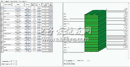
Figure 2 Design of laminated structure
2.2 Power supply design
The noise situation of GTP analog power supply is one of the important factors that affect the performance of GTP. In addition to designing the stack, let the three analog power supplies of GTP be distributed on a separate plane and coupled with the ground plane for coupling. In addition, a magnetic bead is connected in series for each power supply pin, and a 0.22 is connected in parallel. The capacitance of μf forms an LC low-pass filter to filter the power supply. The analog power of GTP is supplied by the low-noise LDO power chip TPS74401, and the output voltage ripple is less than 50mV.
2.3 Clock design
The reference clock of the high-speed serial transceiver is another important factor affecting the quality of signal transmission. This system uses the clock synthesis chip LMK03001C with powerful clock clean function to generate the reference clock of the serial transceiver. The maximum root-mean-square jitter (RMS jitter) of the output clock is less than 550fs, and the duty cycle is 50%. The output clock level standard has LVDS and LVPECL. The frequency of its output clock can be flexibly programmed to meet the requirements of different transmission rates, so that the system can adapt to the realization of multiple serial transmission protocols.
2.4 Pre / de-emphasis and equalization parameter design
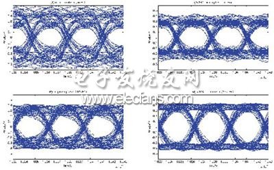
In order to counteract the excessive attenuation of high-frequency components by the transmission path, it is necessary to perform pre-emphasis at the sending end or add equalization at the receiving end or use both methods. Both pre / de-emphasis and linear equalization improve the quality of the received signal through distortion of the signal. Only the appropriate ratio of pre- / de-emphasis and linear equalization and the combination between the two can achieve the purpose of improving the quality of the received signal, otherwise Instead, it will deteriorate the quality of the received signal. This article uses the SPICE model of GTP and the S-parameter model of the serial transmission channel to simulate the transmission quality of the serial link under different pre / de-emphasis and equalization parameter settings, so as to find the appropriate parameter settings.
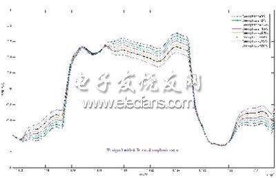
Figure 3 Transmitted signals at different pre / de-emphasis ratios
Figure 3 shows the simulation results under different pre / de-emphasis specific gravity settings. The middle part shows the transmission waveform of three consecutive high-level bits. Obviously, the amplitude of the latter two high-level bits decreases correspondingly with the pre / de-emphasis ratio. In addition, the signal level in the same logic bit in the figure is not flat. This phenomenon is mainly caused by the emission caused by the impedance mismatch on the signal transmission link, such as the connector of the ATCA single board and the ATCA backplane. Junction.
Hair Twist Sponge/Magic Hair Twist Sponge
Product Description:
1. 100% brand new and high quality
2. Twist hair brush sponge3. Like nudred or magic twist brush
4. Great way to get dreads and twists!
5. Save money and time by using this great new styling product.
6. Material: EVA + Sponge

Hair Twist Sponge,Hair Curly Sponge,Men Hair Curly Sponge,Women Hair Curly Sponge
Shenzhen Greater Industry Co., Ltd. , https://www.szgreater.net