Low-noise amplifier (LNA) is an important part of the RF transceiver, it can effectively improve the receiving sensitivity of the receiver, and thus improve the transmission distance of the transceiver. Therefore, whether the design of the low noise amplifier is good is related to the communication quality of the entire communication system. This article takes the transistor ATF54143 as an example to illustrate the design methods of two different low-noise amplifiers. Its frequency range is 2 ~ 2.2 GHz; the operating voltage of the transistor is 3 V; the operating current is 40 mA; the input and output impedance is 50Ω.
1 Qualitative analysis
1. 1 Transistor modeling
You can check the relevant information of the transistor manufacturer through the network, you can download the transistor model provided by the manufacturer, or you can download the S2P file of the tube according to actual needs. In this example, the S2P file of the tube is directly imported into the software, and the circuit is designed using the S parameter as a model. If it is the first time to import, you can use the module SParams to perform S-parameter simulation, observe whether the obtained S-parameter is the same as the data provided by the S2P file, at the same time, measure the input impedance of the transistor and the corresponding minimum noise figure, and determine the stability of the transistor Sex, etc., prepare for the next step.
1. 2 Transistor stability
After completing the S-parameter simulation of the circuit, it can be obtained that the mu of the input / output terminals is less than 1 between 2 and 2.2 GHz. According to RF-related theory, the transistor is unstable. By connecting a 10 Ω and 5 pF capacitor in parallel at the output, the values ​​of m2 and m3 are both greater than 1, as shown in Figures 1 and 2. The transistor achieved stable conditions within the bandwidth, and the input impedance measured at 2.1 GHz was 16.827- j16.041. At the same time, it was found that due to the addition of a resistor at the output, Fmin increased from 0.48 to 0.773, Topt was 0.329 ∠125.99 °, Zopt = (30.007 + j17.754) Ω. Among them, Topt is the best source reflection coefficient.
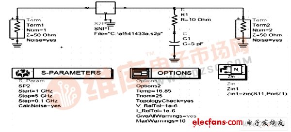
Figure 1 Schematic diagram of circuit simulation using module SParams
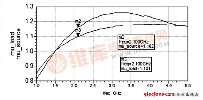
Figure 2 Relationship between input / output mu and frequency
1. 3 develop a plan
As shown in Figure 3, the available gain circle family and noise figure circle family are drawn on the same Ts plane. According to the analysis, if the available gain circle passes the position of the point where the best noise figure is located, and the input end circuit is matched according to this point, then for the LNA, the noise figure is the smallest, but the gain does not reach the most Better zoom. Therefore, it is obtained by sacrificing the available gain. In this case, the transistor gain can reach about 14 dB, Fmin is about 0.48, as shown in Figure 3.
Another solution is to achieve a balance between the available gain and noise figure, with the goal of matching as little noise as possible, and adopt a design solution that takes into account the gain. In this case, the transistor gain is about 15 dB, and Fmin is about 0.7 (see Figure 3). This is the second solution mentioned in this article.
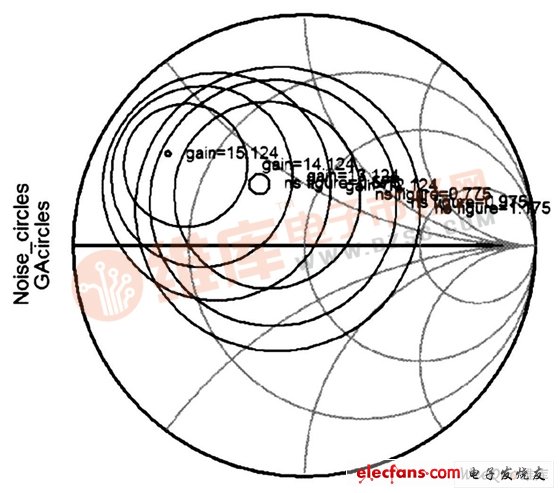
Figure 3 The available gain circle family and noise figure circle family on the same Ts plane.
2 Simulation with the best noise figure as the design target
2. 1 input matching circuit design
For a low-noise amplifier, in order to obtain the minimum noise figure, Ts has an optimal Topt coefficient value, at which time the LNA reaches the minimum noise figure, that is, the best noise matching state. When the matching state deviates from the optimal position, the noise figure of the LNA will increase. In the previous qualitative analysis, Topt = 0. 329∠125. 99 °, and the corresponding Zopt = 30. 007 + j17. 754 Ω have been obtained. Below, you can use ADS's Passive CIRcuit / MicorST rip Window window to automatically generate the matching circuit of the input port.
Add a DA_SSMatch1 smart module to the schematic, and then modify the settings: F = 2. 1 GH z, Zin = 50Ω. It is worth noting that when using this tool to generate a matching circuit, Zload is the conjugate of Zopt. After setting, add another MSub control, which is mainly used to describe the basic information of the substrate. Modify the settings to H = 0.8 mm, Er = 4.3, Mur = 1, CONd = 5.88 & TImes ; 107, Hu = 1. 0e + 33 mm, T = 0.03 mil. After setting, the automatic matching circuit can be generated, and the resulting circuit is shown in Figure 4.
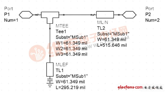
Figure 4 Input port matching circuit
Add the input matching circuit to Figure 1 and then perform S-parameter simulation. It can be seen that the position of the best noise figure Topt is successfully matched to the position of 50Ω due to the addition of the input matching circuit.
2. 2 output end matching circuit design
Design the output matching circuit according to the principle of maximum power gain (considering the presence of the output stabilizing circuit and the impact on the output impedance, the stabilizing circuit must be taken into account when measuring the output impedance), that is, the output impedance (Zout = 8. 055- j8. 980, as shown in Figure 5) Use the above method to match to 50 Ω. The resulting output matching circuit is shown in Figure 6.
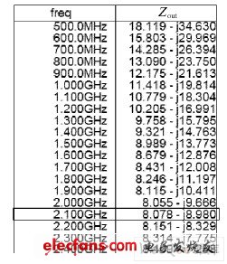
Figure 5 Output impedance matching
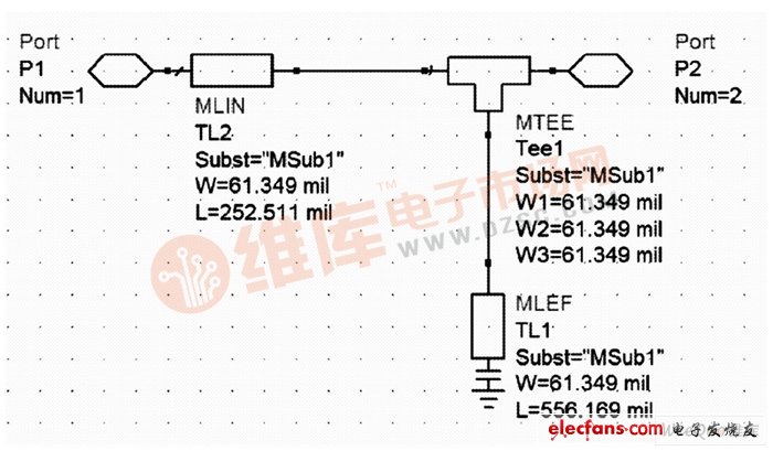
Figure 6 Output matching circuit
2. 3 simulation results
Observing the final simulation results, we can see that the gain is 14.4 dB; the noise figure is 0.586, which is very close to the optimal noise figure of the stabilized transistor of 0.573, and the gain flatness is low, and the stability is excellent. Specific performance indicators are shown in Figure 7.
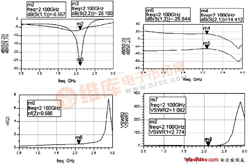
Figure 7 Schematic simulation data
3 Simulation with noise figure as the main target and gain as the design target
3. 1 input matching circuit design
If the substrate material is epoxy glass FR4 substrate, the dielectric constant is 4.3, and the thickness is 0.8 mm, then the input impedance of the transistor at 2.1 GHz is 16.827- j16.041. Using the above matching circuit generation method, the input matching circuit is designed using a single-node module in the A DS design wizard. The matching circuit in Figure 8 can be quickly obtained. As shown in Figure 9, m6 = 50 (0.927 + j0. 001) in the figure. It is very close to 50Ω, so the matching condition of the input terminal is more reasonable.
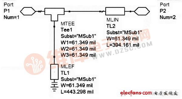
Figure 8 input matching circuit
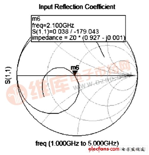
Figure 9 The original diagram of smit h of S 11 after adding the input matching circuit
3. 2 output matching circuit design
After the input matching circuit design is completed, the output matching circuit can be designed. Here, give full play to the advantages of CAD software, with the help of optimized methods to achieve. The basic process is as follows:
Add the result of the input matching circuit to Figure 10, and add the microstrip as shown in the figure at the transistor output. Bring up the optimization control, and set the optimization target to dB (S) 11)) to -20, and dB (S (22)) to -15.
At the beginning of the optimization, first set the width of T L1, T L2, TL3 to 61.394 mil, this is to ensure that the characteristic impedance of the microstrip line is 50 Ω when considering the plate, plate thickness and other factors. The lengths of T L1, T L2, and TL3 are preset. After optimizing once, the results are refreshed. Observe whether the indicators of various charts are better and whether the values ​​reach the set maximum value. If the value reaches the maximum value, change the setting value again to optimize again. After repeated many times, these values ​​will be changed again. If the changes have little effect on various indicators, you can try to change the resistance and input matching values ​​before optimizing.
Through many debugging, it is found that R1 is set to 15Ω, and after adding TL7, the gain and noise figure and the input and output standing wave ratio are better. The schematic diagram of the simulation circuit, the optimization control and the target control are shown in Figure 10.
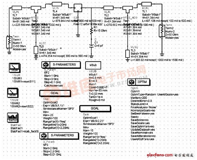
Figure 10 Schematic diagram of simulation circuit and optimization control and target control
3. 3 Simulation results
Observing the final simulation results, we can see that the gain is 15.816 dB; the noise figure is 0.708, which is better than that in qualitative analysis. Other performance indicators are shown in Figure 11.
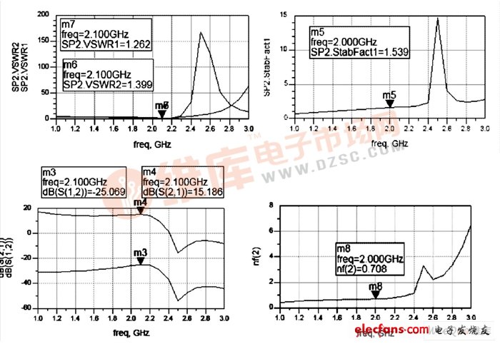
Figure 11 Schematic simulation data
4 Conclusion
Through the qualitative analysis of the transistor, the design scheme of the low-noise preamplifier can be selected according to the actual needs. The best noise figure of the first scheme is obtained at the expense of gain; the second scheme is at the cost of improving the noise figure, It is obtained by lowering the value of standing wave ratio VSWR. Both methods can be realized quickly using computer-aided design tools, and each has its own value, which has been applied in many occasions.
[WATERPROOF] IPX4 waterproof rating protected against splashing water from all angles. you can also doing outdoor activities or excises when raining or snowing.
[LONG BATTERY LIFE] The Head Lamp lighting time up to 8 hours. Whether you're out in remote areas, work in underground or stuck in the highway, applies to a variety of night activities to make your night life easier.
[EASY TO USE]Easy open the head lamp battery case, this led headlight use AAA batteries or rechargeable battery. Durable elastic headband makes hands free.
[WIDELY APPLICATION RANGE]This head Lamp can be used for running, camping, hiking, hunting, fising, climbing, biking, cycling, shooting, caving, kayaking, housing, construction work, auto repair, walking dog at night hands-free,etc
Head Lamp
Head Light,18650 Head Lamp,Zoomable Head Lamp,Head Lamp
Ningbo Henglang Import & Export Co.,Ltd , https://www.odistarflashlight.com